
Designing Antenna-Friendly Enclosures for ESP32-S3: RF Clearance, Wall Thickness, and Material Loss
Jerome Privott · · 5 min read
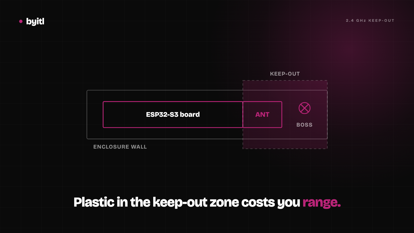
You designed an ESP32-S3 board, verified Wi-Fi and Bluetooth on the bench, and printed a tight-fitting plastic enclosure. But the moment the case snaps shut, RSSI drops by 10 dB, packets start dropping across the room, and your BLE connection drops every time someone walks past.
What happened?
Plastics are not invisible to radio waves. Enclosing an antenna in a 3D-printed shell introduces dielectric loading, detuning, and signal attenuation. Here is how RF energy interacts with 3D-printed plastics, and the exact mechanical rules to keep your ESP32-S3 enclosure antenna-friendly.
The Short Answer
- Keep 3 mm to 5 mm of air space between the PCB antenna element and the inner plastic wall.
- Do NOT put plastic directly against the antenna. Touching the PCB trace antenna shifts its resonant frequency away from 2.4 GHz.
- Avoid Carbon Fiber (CF) filaments completely. CF-PLA and CF-PETG contain conductive carbon strands that act as an RF shield.
- Keep wall thickness near the antenna to 1.2 mm–1.6 mm. Thicker plastic increases dielectric attenuation.
- Keep metal hardware out of the antenna hemisphere. Screws, heat-set inserts, battery leads, and copper fills must stay outside the keepout zone.
1. Dielectric Loading: Why Plastic Detunes Antennas
PCB trace antennas—such as the inverted-F (IFA) or meandered IFA antennas used on ESP32-S3-WROOM modules—are tuned to resonate at 2.4 GHz in free air (relative permittivity $\epsilon_r = 1.0$).
When you place a solid plastic wall right against the antenna, the electric field passes through a medium with a higher dielectric constant:
- PLA: $\epsilon_r \approx 2.7 - 3.2$
- PETG: $\epsilon_r \approx 2.6 - 3.0$
- ABS / ASA: $\epsilon_r \approx 2.5 - 2.8$
- Resin (SLA): $\epsilon_r \approx 3.0 - 3.5$
Because the effective dielectric constant surrounding the antenna increases, the velocity factor decreases, and the resonant wavelength shortens. In practice, touching plastic to an unshielded IFA antenna detunes its center frequency downward—shifting it from 2.45 GHz down to 2.15 GHz - 2.25 GHz.
At 2.44 GHz (Wi-Fi Channel 6 / BLE), the antenna is no longer resonant. Voltage Standing Wave Ratio (VSWR) spikes, transmitter power is reflected back into the ESP32 RF front-end, and receiver sensitivity plunges.
The Mechanical Fix: Air Clearance
Leave a minimum of 3.0 mm (preferably 5.0 mm) of clear air gap between the top, bottom, and edges of the antenna trace and the inside wall of the enclosure. Air maintains $\epsilon_r \approx 1.0$ in the near-field reactive zone of the antenna.
2. Filament Selection: Safe vs. Signal-Killing Plastics
Not all 3D printing filaments behave identically at 2.4 GHz. Your choice of material and additives dictates RF loss.
| Filament Material | $\epsilon_r$ (2.4 GHz) | Loss Tangent ($\tan \delta$) | RF Performance Rating |
|---|---|---|---|
| Natural / White PLA | ~2.7 | ~0.009 | Excellent |
| PETG (Clear / Solid) | ~2.6 | ~0.012 | Good |
| ABS / ASA | ~2.5 | ~0.007 | Excellent |
| Polycarbonate (PC) | ~2.8 | ~0.009 | Good |
| CF-PLA / CF-PETG | Conductive | N/A | ❌ DESTROYS SIGNAL (Shielding effect) |
| Black Filaments (Heavy Carbon Black) | ~3.1 | ~0.025 - 0.040 | ⚠️ Moderate Attenuation |
The Carbon Fiber Trap
Carbon fiber reinforced filaments (CF-PLA, CF-PETG, PA-CF) are extremely popular for rigid enclosures. However, the chopped carbon fiber strands create a conductive percolating network. Placing an ESP32-S3 inside a CF-PETG enclosure is equivalent to putting it inside a mesh Faraday cage. Expect 15 dB to 30 dB of signal loss.
Carbon Black Pigments
Dark black filaments often use carbon black pigment for coloring. High concentrations of carbon black increase dielectric loss tangent ($\tan \delta$). If maximum RF range is critical, use natural, white, or light-colored PETG/PLA around the antenna region.
3. Wall Thickness & RF Windows
RF attenuation increases linearly with wall thickness. A solid 3.0 mm enclosure wall attenuates 2.4 GHz signals significantly more than a 1.2 mm wall.
Recommended Design Rules:
- Standard Enclosure Wall: 2.0 mm for structural rigidity.
- Antenna RF Window: Pocket out the enclosure wall directly over the antenna to 1.2 mm - 1.5 mm thickness.
- 3D Print Infill Pattern: In the area surrounding the antenna, use 100% solid infill or 0% (hollow). Avoid gyroid or grid infill directly over the antenna element, as internal air/plastic lattice voids create unpredictable phase boundaries.
4. Metallic Hardware & Keepout Zones
An antenna's radiation pattern is easily distorted by nearby conductors. Metal objects inside the near field act as parasitic reflectors or ground planes.
Keepout Rules for ESP32-S3 Enclosures:
- Heat-Set Inserts & Screws: Keep M2/M3 brass inserts at least 8 mm away from the antenna trace.
- LiPo Batteries: Lithium pouch batteries have an aluminum/copper foil casing. Placing a battery directly under the PCB antenna will short out the radiation pattern. Position the battery under the MCU/power section, never under the antenna.
- Display Ribbons & Wires: Route power and FPC cables away from the antenna overhang.
- Internal Ribs & Stiffeners: Do not run structural plastic ribs across the top of the antenna PCB section.
Summary Checklist for ESP32-S3 Enclosures
- ✅ Maintain 3 mm–5 mm air clearance above and around the antenna PCB trace.
- ✅ Pocket wall thickness down to 1.2 mm–1.5 mm over the antenna zone.
- ✅ Use standard PETG, PLA, or ABS (avoid Carbon Fiber filaments entirely).
- ✅ Keep screws, brass inserts, and LiPo batteries outside the antenna keepout hemisphere.
- ✅ Ensure the PCB antenna extends to the edge of your internal mounting bosses.
Need a custom ESP32, RP2040, or STM32 enclosure designed and board-verified? At byitl, we build parametric 3D-printable enclosures in 72 hours for a $1,500 flat fee—complete with print-ready STLs and editable STEP files.
Related
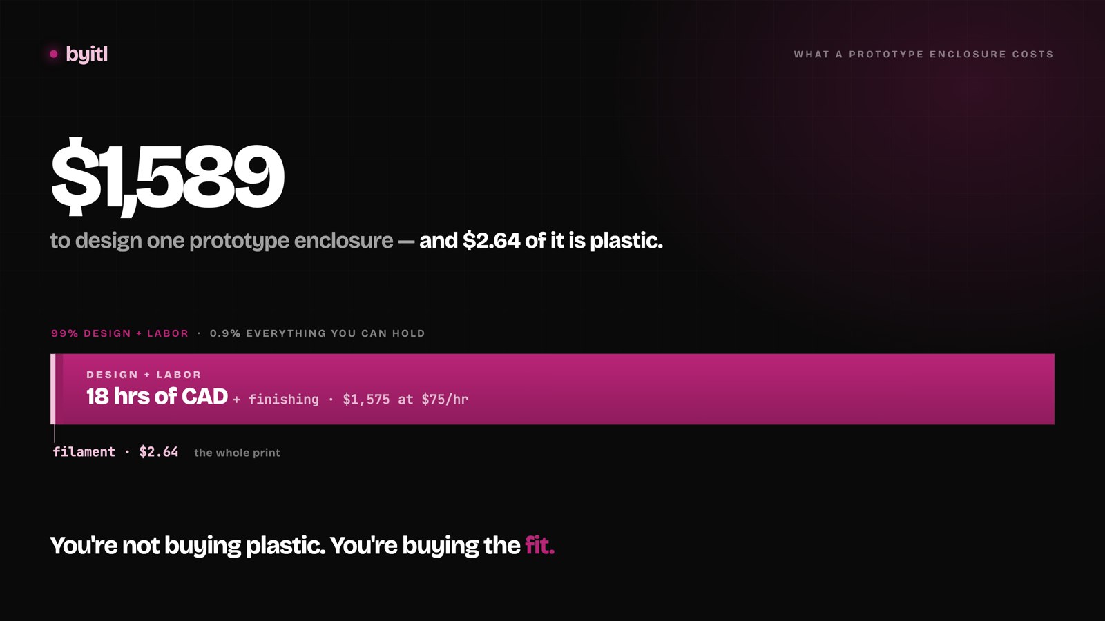
What a 3D-printed prototype enclosure actually costs in 2026
Filament is under half a percent of the bill. Here's the itemized total for a palm-sized ESP32 enclosure, design time included.
· 11 min read
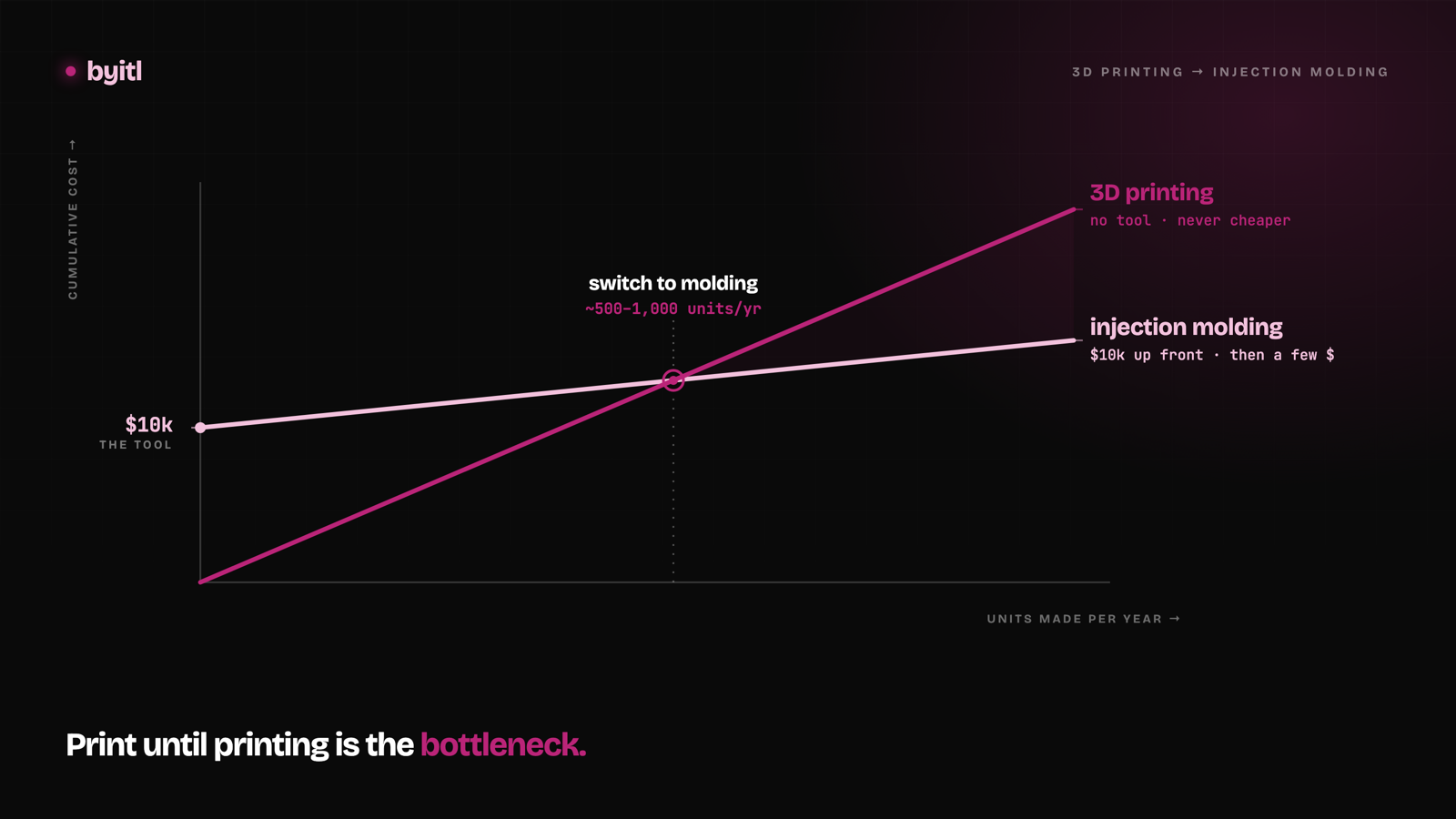
From 3D-printed enclosure to injection molding: when to switch
A single-cavity prototype steel tool for a palm-sized enclosure runs about $10k — we've had our own parts quoted. Here's the break-even math on when it pays.
· 10 min read
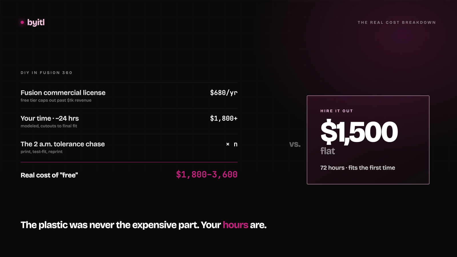
DIY your enclosure in Fusion 360 vs. hiring it out — the real cost breakdown
DIY in Fusion 360 is right for some founders. Here's the exact line where it stops being cheaper — license terms, tolerance stacks, real hours.
· 8 min read