
We told the fab the missing annular rings were intentional. They weren't.
Jerome Privott · · 7 min read
In part one I wrote that JLCPCB caught two things during review before they built anything, and that one of them was whether the removed bottom annular rings were acceptable. I confirmed they were. I described it as an intentional design choice.
That was wrong. We never chose it. I want to correct that here, because the thing I waved through turned out to be the reason only the through-hole joints failed.
What I actually approved
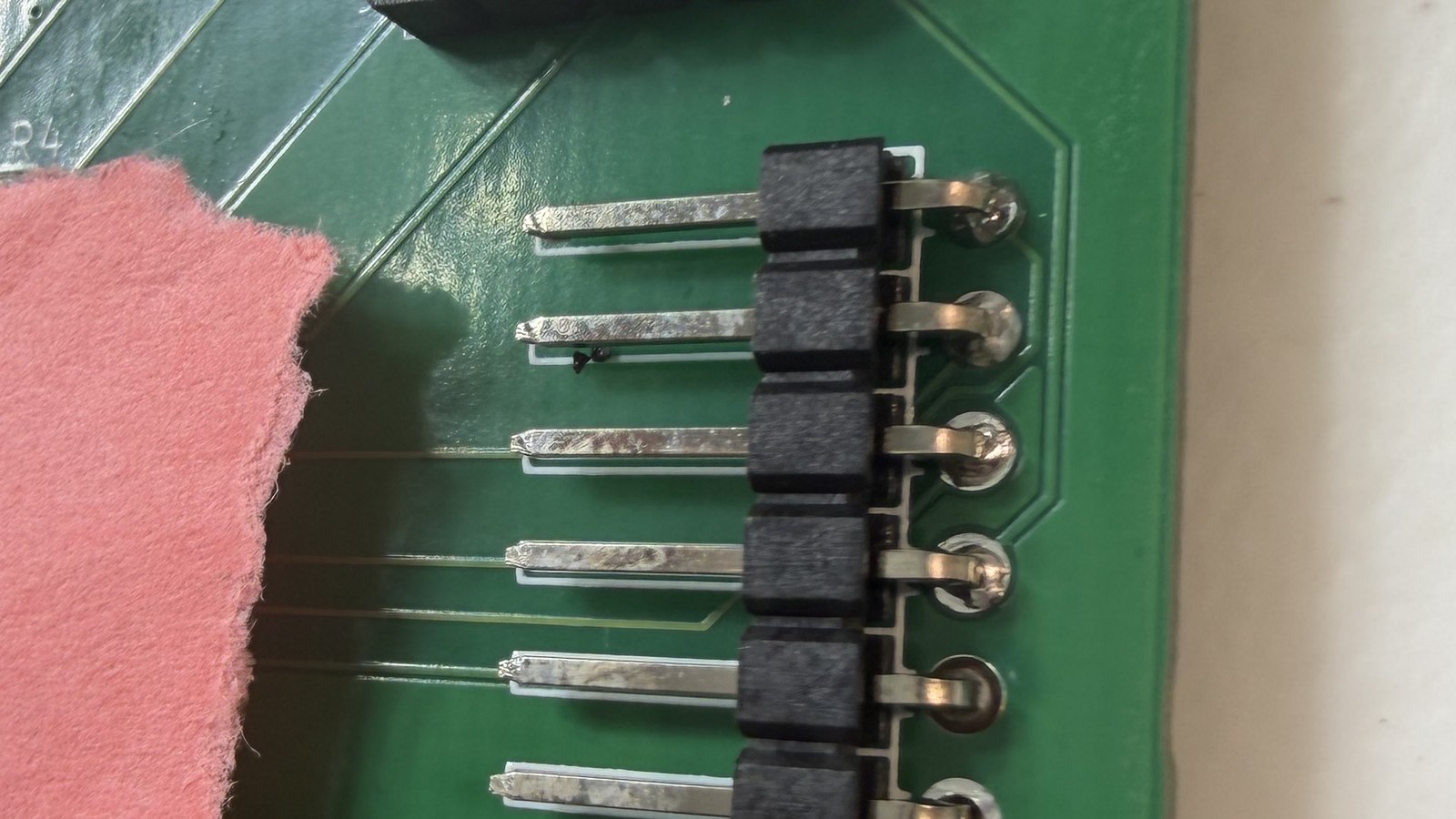
Their reviewer asked about three parts, all connectors, all through-hole. On each one the bottom annular ring had been removed: the plated barrel was intact, the top pad was intact, and there was no copper at all on the solder side.
I looked at the file, saw the flag set, assumed a previous version of me had set it for a reason, and said yes. That is the entire decision-making process, and it is worth being honest about how little there was to it. A vendor asked a good question, and I answered it from the file rather than from intent.
Why it matters more than it sounds
A through-hole joint is not solder sitting on a pad. It is solder wicking the length of a plated barrel and forming a fillet on both sides of the board. The solder-side fillet carries most of the mechanical strength and much of the electrical reliability.
To form that fillet, solder needs a pad on the solder side to wet. Copper it can flow onto and hold. Remove that pad and there is bare soldermask and the mouth of a barrel. The joint can still come out fine when everything goes right. But when a barrel does not completely fill, nothing anchors what is there, and the result reads open on a meter while the connector still looks perfectly placed from above.
Part one's argument was that varying failures across boards from one panel prove process variation. That still holds and I stand by it. What I missed was the question sitting next to it: why was every single failure on a through-hole part, when thirty-one surface-mount components went through the same oven on the same boards without a single defect?
An inconsistent process scatters its failures. Ours correlated perfectly with one attribute. That is not luck. That is a design characteristic removing all the margin from one class of joint.
The flag
Here is the pad, straight out of the board file we sent to be manufactured:
(pad "4" thru_hole circle
  (at 0 7.62)
  (size 1.7 1.7)
  (drill 1)
  (layers "*.Cu" "*.Mask")
  (remove_unused_layers yes)
  (keep_end_layers no)
  (net "DISP_MOSI")
)
remove_unused_layers yes tells KiCad to delete copper on any layer where the pad has no connection. On a two-layer board with a net routed only on top, that deletes the bottom annular ring. It is a genuinely useful feature on multilayer boards, where dead inner-layer rings are wasted copper. On the outer layer of a two-layer board carrying a through-hole connector, it removes the pad you solder to.
Nobody set it
KiCad's own footprints ship with it turned off. Open PinHeader_1x07_P2.54mm_Horizontal.kicad_mod from the standard library and every pad reads:
(remove_unused_layers no)
Our board files are generated programmatically. The library in that pipeline parses pads like this:
if item[0] == 'remove_unused_layers': object.removeUnusedLayers = True
if item[0] == 'keep_end_layers':      object.keepEndLayers = True
Read it slowly. It tests whether the token is present. It never looks at the value. KiCad's own (remove_unused_layers no) contains the token, so loading a stock footprint sets the flag to True. The file said no. The parser heard yes.
The write path completes it. It emits a valueless token:
rul = ' (remove_unused_layers)' if self.removeUnusedLayers else ''
A bare (remove_unused_layers) with no argument is read by KiCad as yes, and canonicalised to (remove_unused_layers yes) on the next write. A setting nobody touched, which the source library explicitly disabled, arrived at the fab inverted.
So when their reviewer asked whether the removed rings were intended, the honest answer was "no, and thank you for asking, let me go find out why they are gone." I did not have the information to give that answer, because everything I could see said the setting was deliberate.
Every gate was green
This is the part worth taking away, because our review process was not lax. It was thorough and it passed the board anyway.
DRC passes. Removing unused layers is legal, intentional KiCad behaviour. There is no violation to report.
ERC passes. Connectivity is fine. Every net reaches its pad on the layer it routes on.
The gerbers are valid. They render cleanly. They are simply gerbers of a board with no solder-side pads.
The 3D render looks perfect, because it renders from the top.
The assembled board looks perfect, because the connector is placed correctly and the top fillet is clean.
The fab's own review flagged it and we told them it was fine.
Nothing anywhere in that chain had an opinion about whether a through-hole pad should have copper on the side you solder from. It became visible on a multimeter, after we had paid for assembly and shipping.
The fix
One line of intent, applied after loading and before writing:
for pad in footprint.pads:
    pad.removeUnusedLayers = False
    pad.keepEndLayers = False
Set the flag explicitly instead of trusting what came back from the parser. We apply it to every placed footprint and every mounting hole now, with a regression test that fails the build if a generated board ever contains the token again, valued or bare.
On the bottom copper layer, same design, same placement, nothing else changed:
- Solder-side pad flashes across the board: 49 before, 59 after
- On the display header alone: 3 before, 6 after
- Top copper and the drill file: essentially unchanged
Ten pads that had no solder-side copper now have it. Three of them are on the header whose pins measured open.
Check your own board in two minutes
You do not need our toolchain to hit this. Any pipeline that round-trips a KiCad file through a library can invert a boolean.
Search the board file.
grep -c "remove_unused_layers yes" yourboard.kicad_pcb
grep -c "(remove_unused_layers)"   yourboard.kicad_pcb
Anything above zero on a two-layer board with through-hole parts is worth a look. The bare valueless form is the more dangerous one, because it does not read as "yes" to a human skimming the file.
Then check the gerbers, not the board file. This is the one that matters, because gerbers are what the fab builds from. Open your bottom copper layer in any gerber viewer and look at the through-hole connectors. Every pin should sit in an annular ring. Bare holes mean you have this problem.
Then check the physical board. Turn it over. Every through-hole pin should sit in solder that has wetted a visible pad, not in a bare hole with a bead sitting in it.
Both things were true
The tidy version of this story is not the honest one, so here is the honest one.
JLCPCB's process was inconsistent. Different pins failed on different boards from the same panel, and no design characteristic explains that. A board with no solder-side pad still assembles reliably under good process control, which is precisely why thirty-one surface-mount parts on those same boards were fine.
And our file gave them nothing to work with. We shipped a design that removed the pad the solder-side fillet needs, on every through-hole pin, on a board whose four most mechanically stressed parts are all through-hole. Then, when asked directly about it before manufacturing, we confirmed it.
Both being true is the normal case in manufacturing failures, not the exception. If we had chased only the vendor half we would have won a refund and then received five replacement boards carrying the identical defect.
How the claim ended
For completeness, because part one left it open.
JLCPCB's engineering team reviewed our documentation and concluded the boards were affected by soldering defects, offering a $15 coupon on that basis on 31 July. On 3 August they offered a $20 refund, again stated as compensation for the soldering defects. On 5 August they withdrew the finding, writing that the earlier conclusion "was based only on the photos you provided, and was an assumption on our side rather than a confirmed finding," and asked for a further round of photographs. After we supplied those, they asked for a further round of resistance measurements, and said an assembly-only refund was proving difficult to secure internally.
At that point we closed the claim and declined the refund. We had been evaluating them as the fabrication partner we would refer client work to, and that is the decision the three weeks actually settled. We will not be recommending them.
We would rather work with a vendor that makes mistakes and holds its findings than one that makes fewer and does not. Every vendor makes mistakes. We made a significant one here ourselves, and it is published above.
What we took from it
Verify on the output artifact. Not the source file, not the review verdict, not the render, and not your own memory of what you intended. The gerbers are what gets built, so the gerbers are what you check. Two minutes looking at the bottom copper layer before ordering would have prevented all of this.
And be suspicious of any boolean that survives a round trip through a library you did not write. This one was set correctly by KiCad, stored correctly on disk, and inverted in the fifteen lines between reading the file and writing it back out.
Related
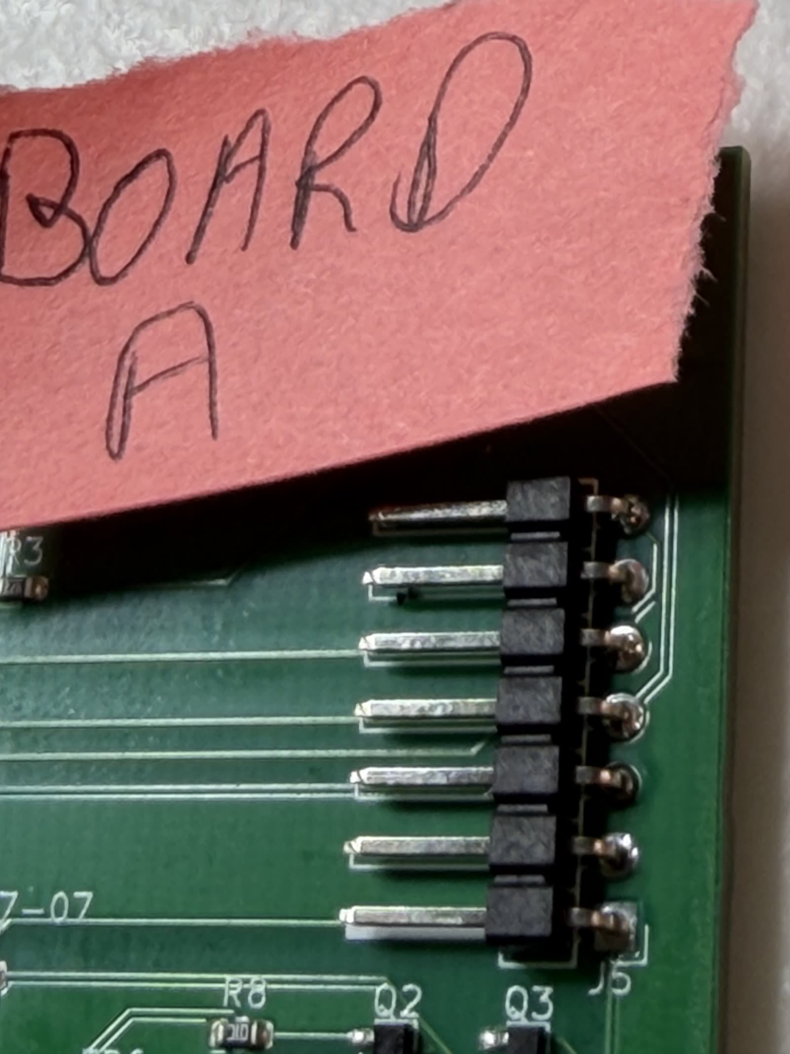
Custom PCB fabrication: three of five boards arrived dead
Three of five assembled boards arrived dead. The defect wasn't ours, and proving that took test points we had added a month earlier.
· 6 min read
We corrected 3.0 mm to 3.175 mm. The calipers read 2.925.
Our spec said 1/8 inch Baltic birch is 3.175 mm. Correct arithmetic on a wrong label. The stock measured 2.925, and the groove was built on the error.
· 6 min read
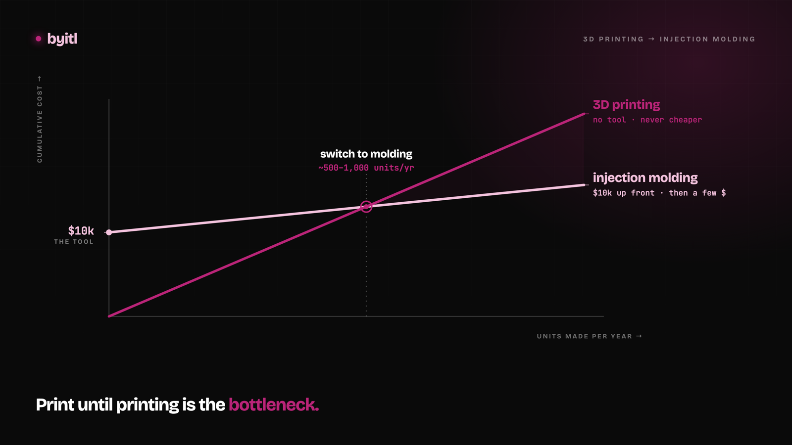
From 3D-printed enclosure to injection molding: when to switch
A single-cavity prototype steel tool for a palm-sized enclosure runs about $10k — we've had our own parts quoted. Here's the break-even math on when it pays.
· 10 min read