
Custom PCB fabrication: three of five boards arrived dead
Jerome Privott · · 6 min read
Five assembled boards arrived from JLCPCB on 16 July. By the following weekend we knew three of them would never power on, and that two of the survivors had a display header only partly connected to the board.
At the time we believed none of it was a design error. For the open display headers that turned out to be wrong; see the update above. Proving the rest took two days — and the reason we could prove it at all was a decision made a month earlier, before the board was ever sent out.
The fab caught two things before they built anything
Custom PCB fabrication has a step people forget about: the fab reads your files back to you.
On 12 July, after the order passed review but before assembly, JLCPCB sent two questions. Which of two soldering profiles was correct for the right-angle header — pins standing at the header's normal standoff height, or bent flat against the surface? And three parts had no pads across part of the bottom layer; was that acceptable?
Both were fair catches. Both were answerable in one email, because we knew why the CAD tool had done it: those pins route only on the top layer, so the unused bottom annular ring gets removed. The holes stay plated through, the top pads are complete. We told them to proceed.
Update, 6 August 2026: This is the part we got wrong. We did not know why the CAD tool had removed those rings, we only assumed we did. Nobody set that option: a parser bug inverted KiCad's own setting and stripped the solder-side pad off the through-hole header pins (J3, J4 and J5), which explains the two open display headers. The three dead boards were a separate fault on the USB-C power path. The fab asked us the right question and we waved it through. Full explanation in part two.
Hold onto that second question. It comes back.
A dead board is not a diagnosis
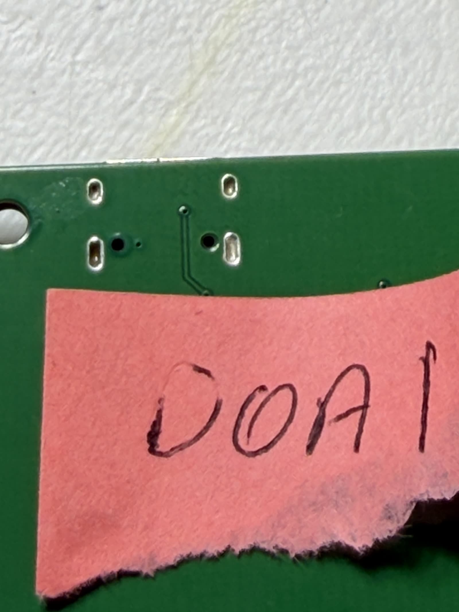
Three of the five did nothing on USB-C. No display, no enumeration on the host.
"Dead" is a symptom, not a finding. The useful question is narrower: where does the voltage stop?
The HC-01 rev D has six test points on the top side. TP1 is the +5 V rail downstream of the F1 polyfuse, TP2 is the +3V3 output of the AMS1117, TP6 is ground. The power path is written down: J6 (USB-C) VBUS → F1 → +5 V (TP1) → U2 AMS1117-3.3 → +3V3 (TP2).
On all three dead boards, using the same cable and the same computer that had flashed a working board minutes earlier, TP1 read 0 V and TP2 read 0 V. The working board read ~5.0 V and ~3.30 V at the same two pads.
One measurement eliminates the cable, the host, the regulator, the firmware, and the schematic in a single move. VBUS never got past the connector.
The second defect only appeared on the boards that worked
Two boards booted normally and drove nothing to the display.
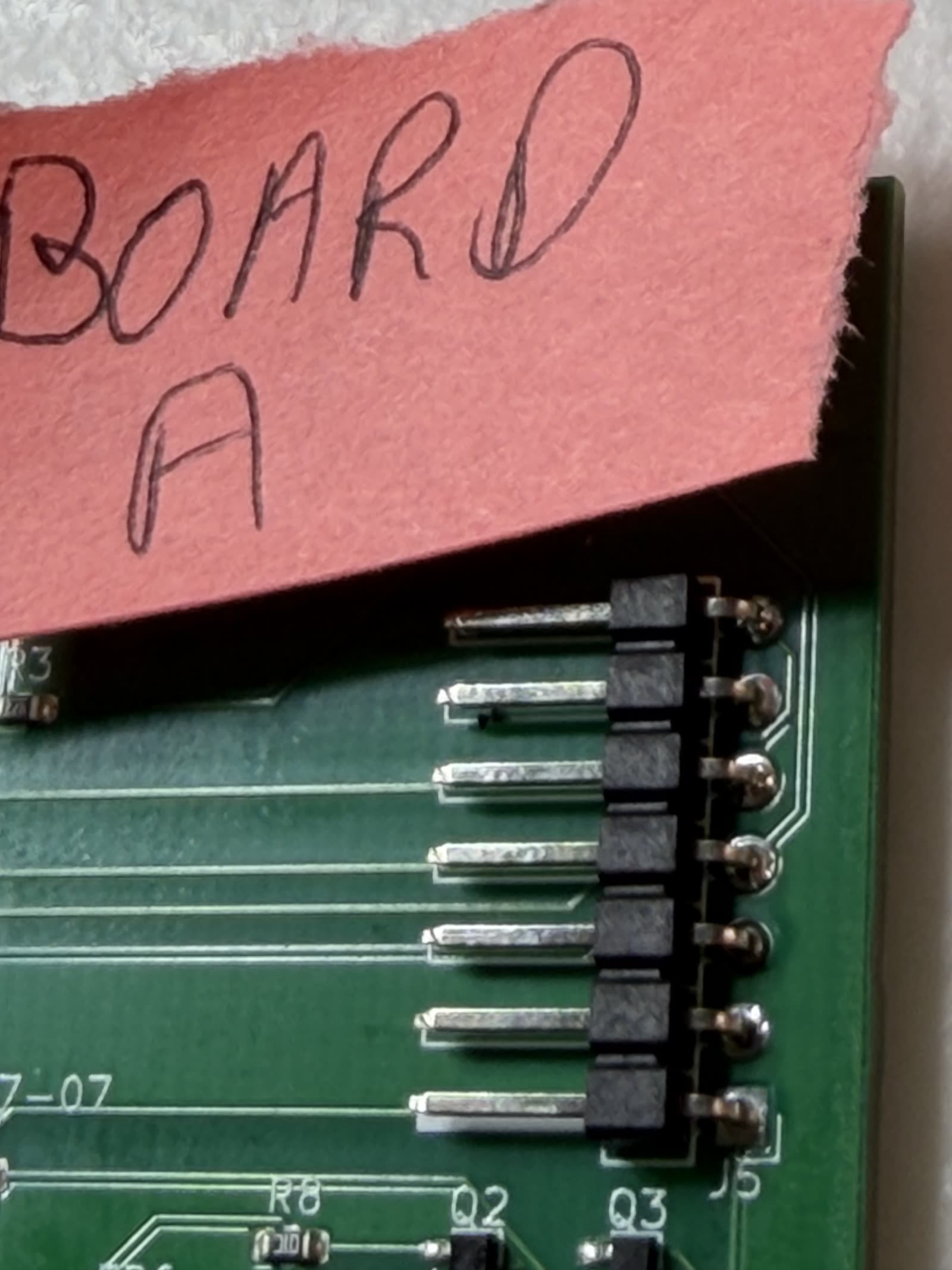
The J5 display header is a 7-pin right-angle part — the same footprint family JLCPCB had asked about on 12 July. Testing it needs no oscilloscope: drive each display net to a steady 3.3 V logic high in firmware, then put a probe on the header pin itself. A good joint reads ~3.3 V. An open joint reads ~0 V.
Two boards, five signal pins, one cable:
- Board A — SCK (3), RES (5) and DC (6) read 3.3 V. MOSI (4) and CS (7) read 0 V.
- Board B — only SCK (3) read 3.3 V. MOSI (4), RES (5), DC (6) and CS (7) all read 0 V.
The variance is the entire argument
If the fault were in our schematic, our footprint, or our firmware, it would fail identically every time. Pin 5 would be dead on both boards or neither.
Instead pin 5 is fine on Board A and open on Board B. Same design file, same panel, same reel, different outcome. That looked like plain process variation. The update above explains why the joint was marginal in the first place.
The photographs agree with the meter: on several pins the solder sits as a dull ball on the pin and never spread into the pad. And the joints on U1 — the ESP32-WROOM-32E module, the part a fab would reasonably suspect first — were clean and properly wetted on every board we photographed.
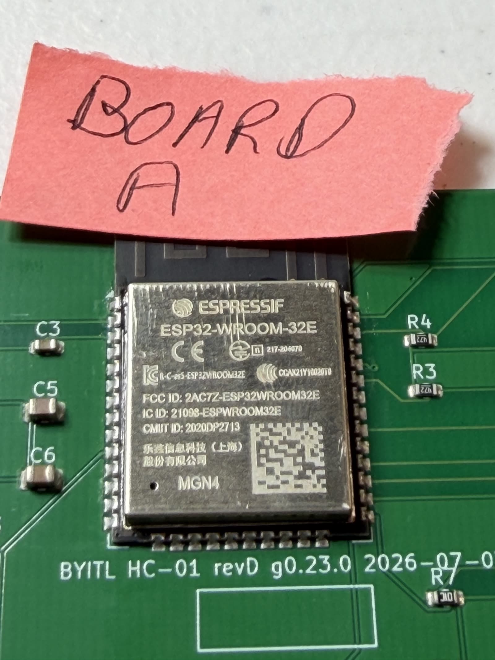
Ruling something out is worth as much as ruling something in. We said so explicitly in the report.
None of this required being clever
It required five things that cost almost nothing at design time:
- Test points on every rail, top side, labeled in silkscreen
- Reference designators you can read without opening the schematic
- The power path written down as an ordered chain, not inferred from a netlist
- A firmware mode whose only job is to make nets measurable
- Board revision and date in the silkscreen, so a photo identifies itself
Without those, the strongest available claim is "some of the boards don't work." That is unanswerable, and a fab cannot act on it. With them, the claim becomes a table of pin numbers and voltages next to a photograph of the joint that produced them.
We call it designing for provable failure. It is not about distrusting the fab. It is about being the person in the thread who can answer the next question immediately.
Prototype planning is one job, not five
JLCPCB responded within hours of the first report, asked for a specific evidence list — connector close-ups, a power-fail video, per-pin measurements, module joint photos — and had it the same day. Two engineers confirmed receipt and the case went to after-sales review; it has since closed. They moved quickly and asked the right questions.
The burden is the interesting part. Answering that list inside a day meant the board, the firmware, and the documentation had already been designed to answer it. For most people those live in five different tools that never talk to each other — schematic capture here, enclosure CAD there, firmware somewhere else, the BOM in a spreadsheet, the fab handoff assembled by hand at 1 a.m.
That is the gap byitl is built to close. One flow from board to enclosure to firmware map to priced BOM to fab handoff, with the bring-up checklist as a gate rather than an afterthought — so the test points, the labeled rails and the measurable nets are in the design before anyone asks you to prove anything.
What we'd tell you before your next order:
- Put test points on every rail and put them on the top side. The one you skip is the one you'll need.
- Write the power path down as an ordered chain. Debugging is walking that chain until the voltage disappears.
- Keep one known-good unit unmodified. Every measurement above is worthless without a reference reading taken on the same cable, minutes apart.
That's the job we do now — board, firmware and enclosure, planned as one thing. See how a full prototype works.
Related
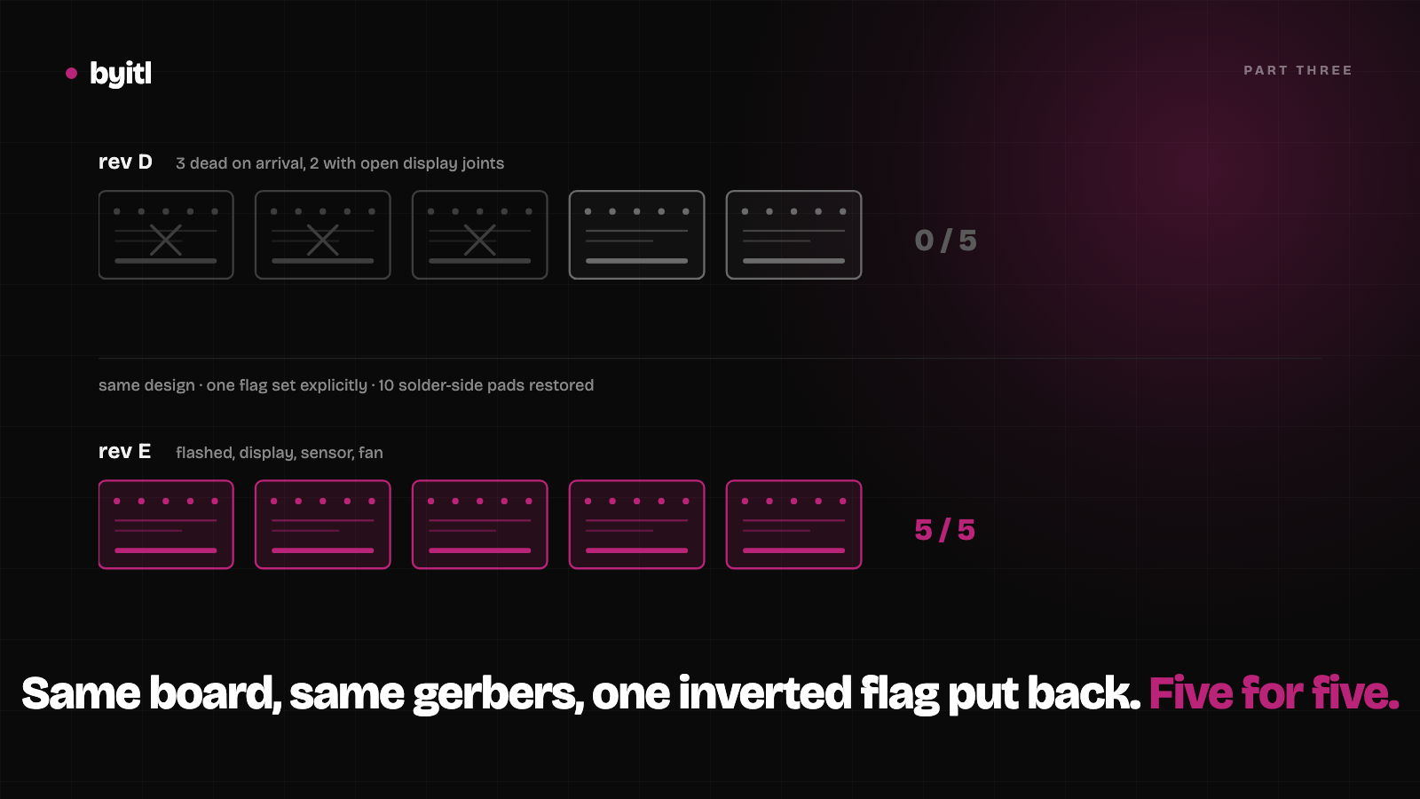
The annular-ring fix held: five of five boards work
Part three. Same design, one inverted flag put back, a different assembler. Five of five rev E boards flashed, drove the display and read the sensor.
· 8 min read
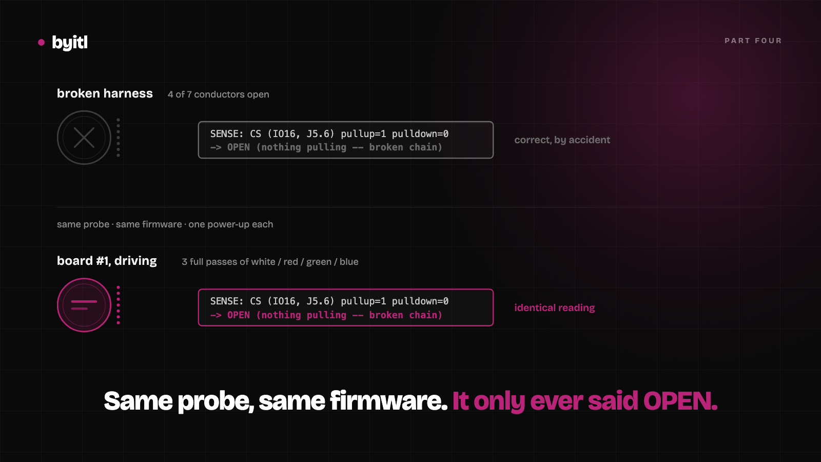
The probe said OPEN. The display was working.
Part four. My J5 continuity probe reported OPEN on a board whose display was provably working, and a bring-up flag shipped on the demo unit.
· 6 min read

We told the fab the missing annular rings were intentional. They weren't.
Part two. The fab asked about one thing before building. We said it was deliberate. It was a parser bug, and it explains the open display headers.
· 8 min read